10 Tips for Reverse Engineering PCBs at the 2026 Canton Fair?
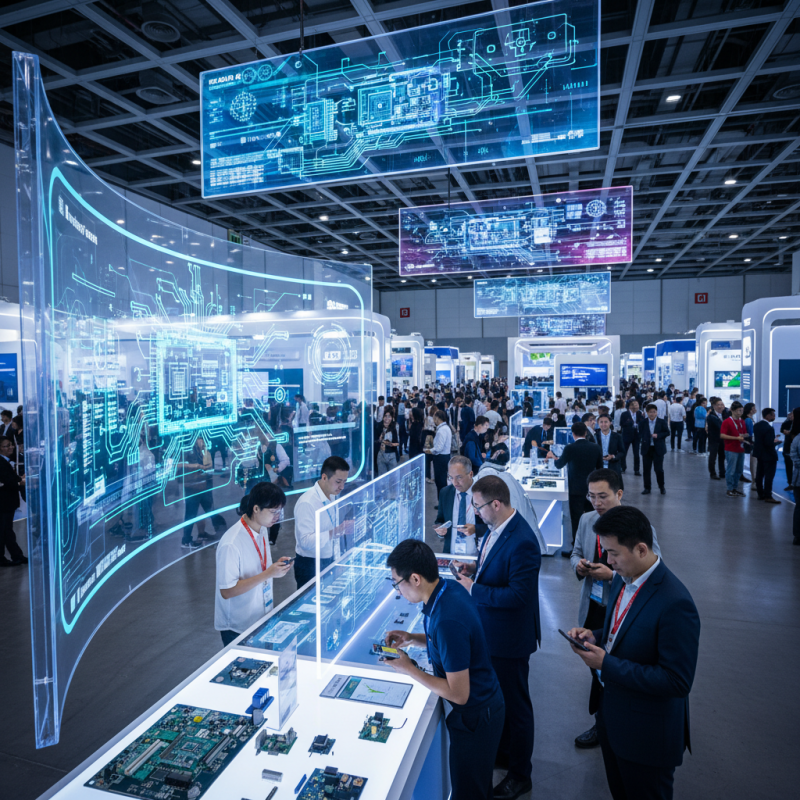
The upcoming Canton Fair in 2026 presents a unique opportunity for enthusiasts of Reverse Engineering Pcb. This event will span from April 15 to May 5, featuring advanced manufacturing and electronics among its focal points. With AI-driven features, attendees can efficiently identify relevant suppliers while navigating a vast exhibition space of 1.55 million square meters.
Reverse Engineering PCB is not only a technical process but also an art. Understanding circuit boards offers profound insights into electronic design. However, this practice comes with its challenges. Many beginners may struggle to grasp the intricate details of PCB layouts and component functions. Mistakes in interpretation can lead to unnecessary failures.
Engaging effectively at the Canton Fair requires preparation. Familiarizing yourself with materials and tools beforehand can greatly enhance your experience. Utilize AI features wisely to connect with the right industry leaders. The fair is a vibrant hub filled with knowledge and innovation, but it’s essential to approach it with a critical mindset. Reflecting on your goals within Reverse Engineering PCB can transform potential frustrations into valuable learning experiences.
Understanding the Basics of PCB Reverse Engineering
Reverse engineering printed circuit boards (PCBs) can be fascinating yet challenging. Many enthusiasts gather to explore this craft, especially at events like the Canton Fair in 2026. Understanding the basics is key to success. Start with the tools you’ll need: a good microscope, soldering iron, and multimeter. These will help you analyze and replicate existing designs. This is where the fun begins.
When dissecting a PCB, carefully document each component. Take notes on values, placements, and connections. Don’t rush; methodical work pays off. You may find some traces are complex and tangled. It’s easy to get lost in the intricacies. If something doesn’t make sense, step back. Analyze your findings with fresh eyes.
In this field, mistakes are learning opportunities. Sometimes, a small oversight can lead to unexpected results. Embrace these moments; they often lead to new insights. The reverse engineering journey is not just about copying but understanding. As you progress, you’ll gain deeper knowledge and skills. This will enhance your appreciation for the craft and might lead to innovative designs of your own.
Essential Tools for PCB Reverse Engineering at Canton Fair
Reverse engineering PCBs can be an intricate process. At the 2026 Canton Fair, having the right tools is critical. A basic toolset should include a magnifying glass. This tool helps inspect fine details on the PCB. A good soldering iron is essential for desoldering components. Choose one with adjustable temperature settings. This will prevent damage to sensitive parts.
You'll also need a digital multimeter. This device measures voltage, current, and resistance. Using it can help troubleshoot circuit issues effectively. It is important to have a PCB design software on hand. This software allows for precise analysis and recreation of the PCB layout. However, the learning curve can be steep for beginners. Practice is essential to mastering these tools.
Don't forget a good set of tweezers. They help handle tiny components with precision. A wire cutter is necessary for trimming excess leads. Be aware that some components may resist removal. You may need several attempts to get it right. Patience is key. Mistakes can happen, so document your process. This reflection can improve your skills for future projects.
Step-by-Step Process of Disassembling a PCB
Disassembling a PCB can be an insightful process, especially for enthusiasts and professionals. Begin by carefully removing any surface-mounted components. This part requires precision; a steady hand can prevent damage. Use a heat gun or soldering iron to melt solder. Make sure to have a magnifying glass handy to catch tiny details.
Next, examine the traces on the board. A digital microscope can reveal hidden connections not visible to the naked eye. According to the IPC's 2023 report, PCB failures mostly occur due to flawed soldering techniques. Understanding these flaws enhances your reverse-engineering skills. It's essential to document each step with photographs for later analysis.
As you continue, keep an eye out for signs of wear or unexpected modifications. These could provide clues about the board's history. The ability to identify these irregularities can be invaluable in your research. It's easy to overlook small things, but they often hold significant meaning. Embrace mistakes and learn from them; not every attempt will be successful. This iterative process fosters growth and deeper understanding in PCB design.
10 Tips for Reverse Engineering PCBs at the 2026 Canton Fair
| Tip Number | Tip Description | Estimated Time | Required Tools |
| 1 | Identify the PCB Type | 30 mins | N/A |
| 2 | Gather Necessary Documentation | 1 hour | Computer, Internet Access |
| 3 | Acquire a Sample PCB | Variable | N/A |
| 4 | Disassemble the PCB | 2 hours | Screwdrivers, Prying Tools |
| 5 | Map Out the Circuit Design | 3 hours | Pen, Paper, Software |
| 6 | Analyze the Components | 1 hour | Multimeter, Datasheets |
| 7 | Create a Schematic Diagram | 2 hours | Circuit Design Software |
| 8 | Document Findings | 1 hour | Text Editor, Diagrams |
| 9 | Prepare a Report | 2 hours | Word Processor |
| 10 | Share with the Community | Ongoing | Social Media, Forums |
Analyzing Components and Schematics in Reverse Engineering
At the 2026 Canton Fair, reverse engineering printed circuit boards (PCBs) presents a unique opportunity for innovation. Analyzing components and schematics is vital for understanding technology trends. Recent industry reports indicate a growth rate of 14% in PCB reverse engineering services. This trend highlights the increasing demand for skilled engineers in this field.
When dissecting a PCB, focus on component identification. Note the placement of capacitors, resistors, and integrated circuits. Proper documentation of these elements aids in creating accurate schematics. Utilize high-resolution imaging tools to capture intricate details. This approach often leads to unexpected discoveries, such as unmarked components or proprietary technologies. Many engineers can miss these nuances, but careful analysis reveals hidden benefits.
Simulating the schematic based on observed components allows for real-time revisions. However, the challenge lies in deciphering complex connections. Misinterpretation can lead to flawed designs. Regularly reviewing your assumptions is crucial. Fine-tuning your approach enhances accuracy and efficiency. Staying updated with evolving technologies ensures that your analysis remains relevant. Acknowledge that reverse engineering is as much about creativity as it is about precision. Each PCB offers lessons, pushing the boundaries of innovation.
Tips for Networking and Learning from Experts at the Fair
Attending the 2026 Canton Fair presents a unique opportunity for networking and learning. Engage actively. Approach experts with genuine curiosity. Ask questions about their experiences and techniques in reverse engineering PCBs. Don't hesitate; most professionals are open to sharing insights.
Focus on building relationships instead of just collecting business cards. During breaks, strike up conversations with nearby attendees. A simple "What are you working on?" can lead to meaningful discussions. Consider participating in workshops to deepen your understanding. Workshops often foster collaboration and idea sharing among attendees.
Reflect on your experiences after each interaction. What went well? What can you improve on? Take notes immediately. You may forget details later. Observing how others network can also provide valuable lessons. Look for styles that resonate with you, but avoid copying directly. Authenticity is key in building lasting connections. Embrace the journey of learning and growing at the fair.
Understanding PCB Reverse Engineering Trends (2026)